DM7406N Datasheet PDF – Hex Inverting Buffer

DM7406N Datasheet PDF learn more.

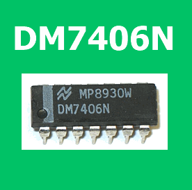
Part number: DM7406N

Functions: Hex Inverting Buffers with High Voltage Open-Collector Outputs.

Package information: SOIC, DIP 14 Pin Type

Manufacturer: Fairchild Semiconductor, National Semiconductor

Image:

DM7406N datasheet pdf

Description

The DM7406 is a hex inverting buffer IC featuring high-voltage open-collector outputs, typically housed in DIP or SOP packages for TTL logic applications. Each of its six independent inverters provides strong sink capability and allows interfacing with higher voltage loads through external pull-up resistors. It is commonly used in level shifting, driving lamps or relays, and general-purpose logic inversion in digital systems.

Features

  • Six independent inverting buffers
  • Open-collector outputs for flexible voltage interfacing
  • High-voltage output capability up to 30V
  • Compatible with standard TTL logic levels
  • High current sinking capability
  • Suitable for driving LEDs, relays, and other loads
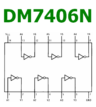
Pinout

DM7406N pinout

Design Notes

  • External pull-up resistors are mandatory for proper output logic levels
  • Pull-up resistor value should be selected based on required speed and load current
  • Suitable for level shifting between TTL and higher voltage systems
  • Ensure output current does not exceed per-channel limits
  • Consider propagation delay in high-speed logic applications

Typical Circuit Usage

  • Driving relays or solenoids from logic signals
  • LED or lamp drivers with higher voltage supply
  • Level shifting from 5V logic to higher voltage domains
  • Wired-OR logic configurations
  • Signal inversion in digital circuits

How to Choose This Part

  • Use when open-collector outputs are required for voltage flexibility
  • Ideal for applications needing higher voltage switching than standard TTL
  • Choose based on required sink current capability per channel
  • Consider external resistor and load requirements in design
  • Evaluate switching speed versus load capacitance

Applications

  • Industrial control logic systems
  • Interface circuits between logic families
  • Display and indicator driving circuits
  • Relay and actuator drivers
  • General-purpose digital logic inversion

Alternative / Equivalent Products

  • SN7406
  • 74LS06
  • 74HC06 (with different logic characteristics)
  • ULN2003 (for higher current array applications)
  • CD4069 (standard inverter, non open-collector)

[ … ]

DM7406N PDF File

download
DM7406N pdf

7404 – Hex Inverting Gates, 14 pin

7404 Datasheet PDF learn more.

Part number : 7404, DM7404, SN74LS04

Functions : Hex Inverting Gate

Package information : DIP, SOP 14 Pin Type

Manufacturer: Fairchild Semiconductor

Image :

7404 datasheet hex inverter

The texts in the PDF file :

DM7404 Hex Inverting Gates

Description

This device contains six independent gates each of which performs the logic INVERT function. Ordering Code: Order Number Package Number Package

DM7404M M14A 14-Lead Small Outline Integrated Circuit (SOIC), JEDEC MS-012, 0.150 Narrow DM7404N N14A 14-Lead Plastic Dual-In-Line Package (PDIP), JEDEC MS-001, 0.300 Wide Devices also available in Tape and Reel. Specify by appending the suffix letter “X” to the ordering code. Connection Diagram Function Table Y=A Inputs A L H H = HIGH Logic Level L = LOW Logic Level Output Y H L © 2000 Fairchild Semiconductor Corporation DS006494 www.fairchildsemi.com DM7404 Absolute Maximum Ratings(Note 1) Supply Voltage 7V Input Voltage 5.5V Operating Free Air Temperature Range 0°C to +70°C Storage Temperature Range −65°C to +150°C Note 1: The “Absolute Maximum Ratings” are those values beyond which the safety of the device cannot be guaranteed. The device should not be operated at these limits. The parametric values defined in the Electrical Characteristics tables are not guaranteed at the absolute maximum ratings. The “Recommended Operating Conditions” table will define the conditions for actual device operation. Recommended Operating Conditions Symbol VCC VIH VIL IOH IOL TA Parameter Supply Voltage HIGH Level Input Voltage LOW Level Input Voltage HIGH Level Output Current LOW Level Output Current Free Air Operating Temperature Min 4.75 2 0 Electrical Characteristics over recommended operating free air temperature range (unless otherwise noted) Symbol Parameter Conditions VI Input Clamp Voltage VCC = Min, II = −12 mA VOH HIGH Level VCC = Min, IOH = Max Output Voltage VIL = Max VOL LOW Level VCC = Min, IOL = Max Output Voltage VIH = Min II Input Current @ Max Input Voltage VCC = Max, VI = 5.5V IIH HIGH Level Input Current VCC = Max, VI = 2.4V IIL LO [ … ]

7404 PDF File

DM7404 pdf
7404 pdf

download