Transistor A1742 Datasheet PDF learn more.
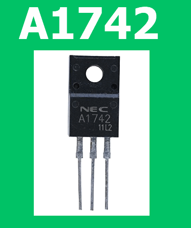
Part number: 2SA1742
Functions: -60V, -7A, PNP Transistor
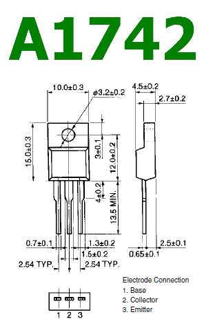
Package information: Isolated TO-220 Type
Manufacturer: NEC
Image:
Description
A1742 transistor is -60V, -7A, PNP Silicon Power Transistor.
The 2SA1742 is a power transistor developed for high-speed switching and features a high hFE at low VCE(sat). This transistor is ideal for use as a driver in DC/DC converters and actuators. In addition, a small resin-molded insulation type package contributes to high-density mounting and reduction of mounting cost.
🧩 Features
- High hFE and low VCE(sat)
- hFE ≥ 100 @ VCE = −2.0 V, IC = −1.5 A
- VCE(sat) ≤ −0.3 V @ IC = −4.0 A, IB = −0.2 A
- Full-mold insulated package (no insulating washer or bushing required)
Pinout
⚠️ Absolute Maximum Ratings (Ta = 25°C)
| Parameter | Symbol | Conditions | Rating | Unit |
|---|---|---|---|---|
| Collector to Base Voltage | VCBO | — | −100 | V |
| Collector to Emitter Voltage | VCEO | — | −60 | V |
| Emitter to Base Voltage | VEBO | — | −7.0 | V |
| Collector Current (DC) | IC | — | −7.0 | A |
| Collector Current (Pulse) | ICP | PW ≤ 300 µs, Duty ≤ 10% | −14 | A |
| Base Current | IB | — | −3.5 | A |
| Total Power Dissipation | PT | TC = 25°C | 30 | W |
| Total Power Dissipation | PT | TA = 25°C | 2.0 | W |
| Junction Temperature | Tj | — | 150 | °C |
| Storage Temperature | Tstg | — | −55 to +150 | °C |
📐 Electrical Characteristics (Ta = 25°C)
| Parameter | Symbol | Conditions | Min | Typ | Max | Unit |
|---|---|---|---|---|---|---|
| Collector Cutoff Current | ICBO | VCB = −40 V, IE = 0 | — | — | −1 | µA |
| Emitter Cutoff Current | IEBO | VEB = −4 V, IC = 0 | — | — | −1 | µA |
| DC Current Gain | hFE1 | VCE = −2 V, IC = −100 mA | 100 | — | 400 | — |
| DC Current Gain | hFE2 | VCE = −2 V, IC = −3 A | 35 | — | — | — |
| Gain Bandwidth Product | fT | VCE = −10 V, IC = −50 mA | — | 150 | — | MHz |
Applications
1. High-Speed Switching
[ … ]
A1742 PDF File


